Basic Demonstrations with BOUNCE
Revised November 1, 2001
1 Introduction
Program BOUNCE demonstrates traveling waves on simple transmission line circuits using animation. This report describes how BOUNCE can be used to introduce students to the basic concepts of “traveling wave”, of reflection from a mismatched load, and transmission onto a line of a different characteristic resistance, and so forth. To familiarize yourself with the operation of the program, read the BOUNCE User’s Guide[1].
The first set of demonstrations show the basic behavior of transmission lines. We start by illustrating wave propagation along a transmission line, and reflection of a pulse from an unmatched load. Further demonstrations look at more complex circuits. Two transmission lines in series illustrate reflection from a junction, and transmission onto the second line. A transmission line with a resistance connected across the center demonstrates reflection from the shunt resistor, and transmission onto the part of the line beyond the resistor. A transmission line that branches into two lines is similar in behavior to the line with the shunt load.
A simple transmission line terminated with a capacitor or an inductor introduces transmission line behavior with energy storage elements. This is then extended to RL and RC circuit terminations.
The transition to the sinusoidal steady state is demonstrated using a sine wave generator. The BOUNCE program shows the development of a standing wave when the load is an open circuit or a short circuit. Also, with a mismatched load, the program demonstrates the concept of “standing wave ratio”.
The reader is intended to run the BOUNCE program in conjunction with the examples presented in the following. The “snapshots” included as figures in this document do not replace moving picture obtained by running BOUNCE for each example.
2
Wave
Propagation
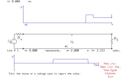
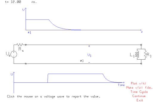
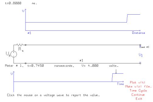
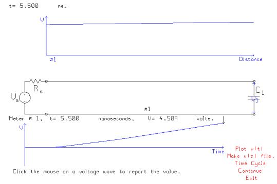
The first built-in circuit or “circuit template” in BOUNCE provides some very basic demonstrations to become familiar with the program and with waves on transmission lines. The circuit is a 2 m transmission line with a phase velocity equal to the speed of light in free space, 300 meters per microsecond or 30 cm per nanosecond, and a characteristic resistance of 50 ohms. The line is excited by a pulse of duration 3.333 ns, corresponding to the period of a 300 MHz clock. The load is matched. There is a “voltmeter” monitoring the voltage near the middle of the transmission line. This problem represents a rather long cable interconnecting a generator or “talker”, a “listener” with a high impedance near the middle of the line, and a load which is matched, all working at a 300 MHz clock speed. The wavelength is 1 m so the interconnecting cable is 2 wavelengths long.
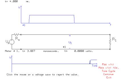
When the circuit is “run” by clicking the “GO” button on the main menu, the pulse advances from the generator along the transmission line. The above drawing shows the pulse at t=4 ns. The leading edge of the pulse has passed the location of the “listener” at voltmeter V1, and the voltage has stepped up to five volts.
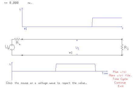
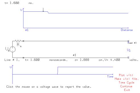
As time advances, the pulse travels to the load and is absorbed because the load is matched. This drawing shows the transmission line at t=8 ns. The trailing edge of the pulse has passed by the “voltmeter” or observer, and the voltage has fallen back down to zero volts. This demonstrates the basic concept of a wave that travels along a transmission line at a constant speed and is absorbed by a load.
Change the generator to a triangle wave using the “Generator” button on the main menu.
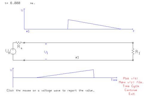
The triangle generator’s voltage rises linearly from zero to five volts and then abruptly falls back to zero. As the voltage rises, the leading edge travels out onto the transmission line. At the voltmeter location, there is a time delay equal to the distance from the generator to the voltmeter divided by the wave velocity, and then the voltage rises linearly to five volts, and falls back to zero. This problem illustrates that the voltage as a function of distance is mirror-imaged compared to the voltage as a function of time.
Change the generator to a sine wave to demonstrate a sinusoidal wave traveling along a transmission line.
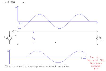
As time advances the sinusoid travels out from the generator and the leading edge advances across the screen. At the voltmeter, there is a time delay during which the leading edge travels from the generator to the voltmeter position, and then the voltage varies sinusoidally with time. Since the load is matched, the sine wave is fully absorbed by the load, so when the leading edge of the voltage reaches the load, the circuit is in the sinusoidal steady state.
3 Reflection from an Unmatched Load
Return to the pulse generator, and change the load to 25 ohms so that it is not matched to the transmission line. When the pulse reaches the load, we have a reflection. The reflection coefficient is
![]()
so the reflected pulse is of amplitude –1.667 volts. The load voltage will be the sum of the incident plus the reflected pulse, 5 plus –1.667 = 3.333 volts.
Run the simulation by clicking “GO”. The leading edge of the pulse travels to the load and then is reflected back. The reflection travels from right to left across the screen, combining with the incident voltage to obtain the net voltage on the transmission line, which is the sum of the incident voltage pulse plus the reflected voltage pulse.
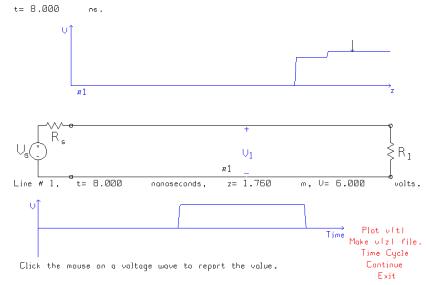
This graph shows the simulation at t=8 ns. You can “read back” values from the graph by clicking the mouse on either the voltage vs. distance waveform, or on the voltage vs. time waveform. To find the voltage at the load, click the mouse on the right hand end of the voltage as a function of distance at the top of the screen. The program reports the voltage by writing text under the circuit schematic; thus the voltage is 3.333 volts, as expected.
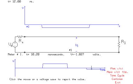
Click the mouse on “Continue” to advance the time by another cycle. As the reflection passes the “voltmeter” in the middle of the line, we see a negative pulse of -1.667 volts.
It is instructive to move the voltmeter to a location close to the end of the line but not quite at the end. First the 5 volt pulse from the source arrives and the voltage steps up to 5 v. Then the –1.67 volt reflected pulse arrives and the voltage steps down to 3.33 volts. Then the 5 volt pulse from the source terminates and the voltage becomes equal to the reflected pulse only, -1.67 volts. Then the reflection ends and the voltage drops to zero.
If we move the observer still closer to the load then the incident pulse and the reflected pulse arrive more nearly at the same instant of time. The length of time that the voltage remains at 5 volts decreases. If the observer is put right at the load, then the incident and reflected pulses arrive exactly at the same time, and the voltage at the observer rises directly to 3.333 volts with no initial peak of 5 v.
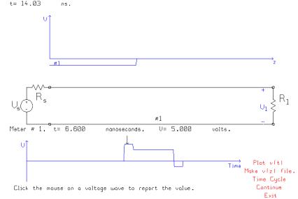
If the load resistor is changed to 75 ohms then the reflection coefficient is +0.2. The reflected pulse’s voltage is then + 1 volt. The drawing above shows the reflected voltage wave of amplitude 1 volt combining with the incident voltage wave of amplitude 5 volts, for a net voltage of 6 volts.
As time advances further, the reflected pulse travels past the location of the observer, and the amplitude can be verified to be 1 volt, as expected.
In general if the load resistance is higher than the line characteristic resistance the reflected pulse has a positive amplitude; if lower then the reflected pulse has a negative amplitude. This is obvious from the formula for reflection coefficient!
4 Unmatched Load, Pulse Train
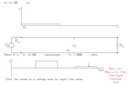
In this demo the source is matched to the 50 ohm line but the load is 25 ohms so is not matched and has a reflection coefficient of –1/3. We will use a square-wave generator or “pulse train” at 150 MHz. We can think of the square wave as a sequence of 1s and 0s to demonstrate the effect of an unmatched load on a bit stream.
Change the generator to a pulse train, and set the frequency to 150 MHz. Reset the number of steps per cycle to 600 so that the BOUNCE program will “run” for a long time before the first pause. The generator launches a series of pulses of amplitude 5 volts onto the transmission line and these are the “positive-going” traveling wave. The load reflects the pulses with a reflection coefficient of –1/3, so the “negative-going” wave is of amplitude –1.667 volts. The voltage on the transmission line is the sum of the positive-going wave and the negative-going wave.
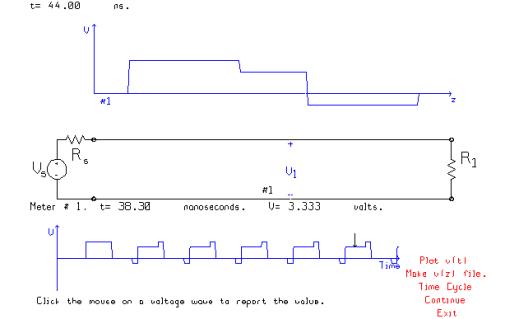
The first pulse to arrive at the voltmeter is of 5 volt amplitude. But subsequent pulses are corrupted by the reflected voltage from the load, of -1.667 volts. The 2nd and subsequent pulses first drop to –1.667 volts as a reflected pulse arrives at the voltmeter; then rise to 3.333 volts as an incident pulse arrives, then rise to 5 volts briefly after the reflected pulse passes. It is instructive to change the location of the voltmeter. The relative timing of the arrival of the incident and reflected pulse depends on the voltmeter’s position, hence the waveform changes with voltmeter position.
5
Transmission
Lines in Series
When two transmission lines are connected in series the first line sees the characteristic resistance of the second line as a “load”. Set the generator to a pulse width of 3.33 ns, 10 volts amplitude and 50 ohm internal resistance. Consider a 1 m, 50 ohm line connected to a 1 m, 25 ohm line, which is terminated in a 25 ohm resistance. The reflection coefficient at the junction is
![]()
hence is ![]() –1/3. When a 5 volt
pulse is incident on the junction, a –1.667 volt amplitude pulse is
reflected. The transmission coefficient
onto the second line is 2/3; hence a 3.333 volt pulse is transmitted onto the
second line. The matched load absorbs
this pulse.
–1/3. When a 5 volt
pulse is incident on the junction, a –1.667 volt amplitude pulse is
reflected. The transmission coefficient
onto the second line is 2/3; hence a 3.333 volt pulse is transmitted onto the
second line. The matched load absorbs
this pulse.
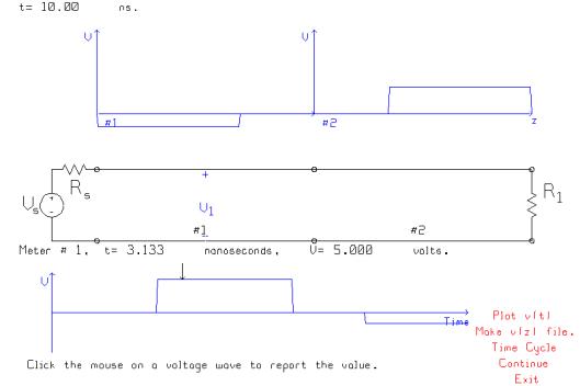
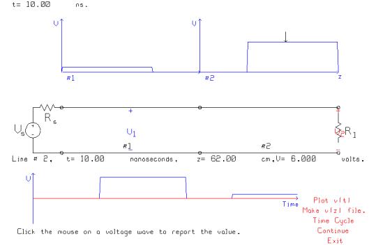
This figure shows the voltage near the middle of the first transmission line as a function of time. First the 5 volt source pulse passes by, and then later the reflected pulse of –1.667 volts amplitude arrives. At t=10 ns, this pulse has not yet passed by the V1 location on the first line. Note too that the 2nd transmission line has a 3.333 volt pulse on it, which has propagated just as far as the load at t=10 ns.
This demonstration can be extended in various ways. First change the 2nd line’s characteristic resistance to 75 ohms. The reflection coefficient is now +0.2 and we can verify that the reflected pulse has amplitude +1 volt. Also, the transmission coefficient is 1.2 and we can verify that the transmitted pulse has amplitude 6 volts.
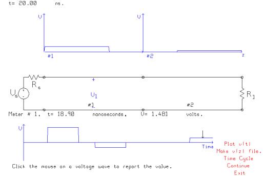
Next restore the second line to 25 ohms, but make the load 50 ohms. The reflection coefficient at the 50 ohm load is 25/75=1/3, so there is a reflected pulse of amplitude 1/3x3.333=1.111 volts on the 2nd line. This travels back to the junction; the transmission coefficient from the 2nd line to the 1st line is 2x50/(25+50)=100/75=4/3, so the transmitted pulse amplitude is 1.481 volts. There is a reflection of the 1.111 volt pulse on the 2nd line back to the load; and a re-reflection back to the junction. This gives rise to a 0.1646 volt pulse at our observer at the middle of the 1st line.
6
Transmission
Line with Shunt Load
Consider a 2 m, 50 ohm transmission line with a matched source and a
matched load. Suppose that a ![]() 50 ohm resister is connected across the center of the
transmission line. This divides the
line into two halves. The left half
sees as its load a 50 ohm resistor in parallel with a 50 ohm transmission
line. The load is thus 50 parallel 50
ohms or
50 ohm resister is connected across the center of the
transmission line. This divides the
line into two halves. The left half
sees as its load a 50 ohm resistor in parallel with a 50 ohm transmission
line. The load is thus 50 parallel 50
ohms or ![]() 25 ohms, and the
reflection coefficient is
25 ohms, and the
reflection coefficient is
![]()
and is –1/3; thus if the incident pulse has amplitude 5 volts the reflected pulse amplitude is –1.667 volts. The transmission coefficient onto the 2nd line is
![]()
which equals 2/3 for our values. We can verify that the transmitted pulse onto the 2nd transmission line is of amplitude 2/3 x 5 volts = 3.333 volts.
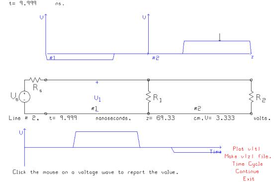
This figure shows the voltage on the transmission lines at t=9.999 ns. Line #2 has a pulse of 3.333 volts amplitude as expected. The shunt load across the transmission line combines in parallel with the characteristic resistance of the 2nd line to make a 25 ohm load, which terminates the first line.
7 Branching Transmission Line Examples
This section deals with transmission lines with branches. The first example is similar to the shunt load problem discussed above. Then an example related to digital logic design is presented.
7.1 Branching to Matched Loads
Consider
a 1 m, 50 ohm line that branches into two 1 m, 50 ohm lines in parallel, each
terminated with a 50 ohm resistor. As
above, the source is matched and generates a 5 volt pulse on the first
line. We will show that this problem
behaves the same way as the previous one.
The first line sees as its load two 50 ohm transmission lines in
parallel, making up a load resistance of ![]() ohms. The reflection coefficient is thus –1/3 as
above and the reflected pulse amplitude is –1.667 volts. The transmission coefficient is identical
to the above, and so has a value of 2/3. We can readily verify that the pulse
transmitted onto either one of the two parallel transmission lines has
amplitude 3.333 volts.
ohms. The reflection coefficient is thus –1/3 as
above and the reflected pulse amplitude is –1.667 volts. The transmission coefficient is identical
to the above, and so has a value of 2/3. We can readily verify that the pulse
transmitted onto either one of the two parallel transmission lines has
amplitude 3.333 volts.
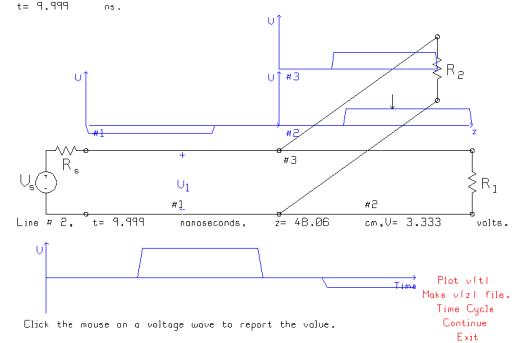
This
figure shows the voltage on all three transmission lines at t=9.999 ns. Line #2 carries a pulse of amplitude 3.333
volts, as expected.
7.2
Short
Branch
This example is based in CMOS logic, where 0 volts is “logical 0” and 5 volts is “logical 1”. The minimum voltage at a gate input for a “logical 1” is 3.8 volts for this type of CMOS gate. Our circuit models a gate driving an 11.5 cm interconnect terminated in another gate that has a 50 ohm matching resistor in parallel. There is a 2 cm branch to the input of a third gate, but there is no matching resistor terminating the branch.
Consider a generator with a 50 ohm internal resistance, which generates a 10 volt pulse lasting 1 ns. It is connected to a 1.5 cm transmission line with 50 ohm characteristic resistance and 20 cm/ns propagation speed. This line branches into two lines, both with 50 ohm characteristic resistance and 20 cm/ns wave speed. One branch is 10 cm long and ends in a 50 ohm matched load. The other branch is short, only 2 cm long, and is terminated Our CMOS gates have an input capacitance of 1 pF, and the rise time of the pulse is 0.1 ns.with a high impedance CMOS gate. We want to know the voltage across the 50 ohm load. Initially we will ignore the input capacitance and the rise time.
To get an insight into this problem, start by using a very short pulse of 0.05 ns length. The generator launches a 5 volt pulse onto line #1, which propagates through the junction and becomes a 3.333 volt pulse on line #2, and a 3.333 volt pulse on line #3. Note that 3.333 volts is not sufficient for a “logical 1”. The pulse coupled into the branch bounces back and forth between the open-circuit load and the impedance mismatch at the junction. Each time it reflects from the junction it launches a pulse on line #2 towards the load.
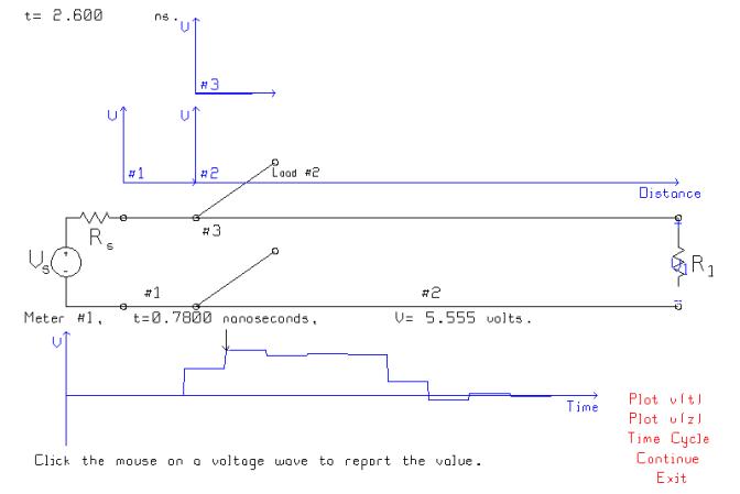
Now change the pulse length to 1 ns. The initial step up in voltage at the load is 3.333 volts, insufficient for a “logical 1”. When the first step from the branch arrives at the load the voltage rises to 5.555 volts, a good “logical 1”. The time required for the load voltage to exceed 3.8 volts is 0.78 ns. Thus the presence of the branch “slows down” the circuit because the load must wait for reflections to arrive from the mismatched branch.
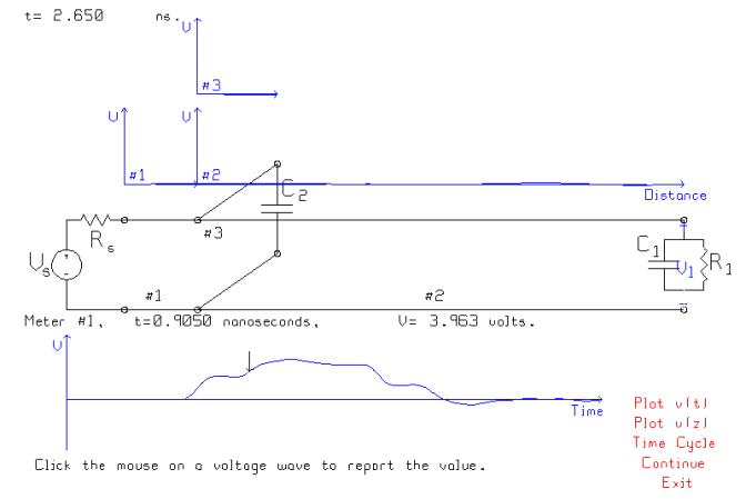
Now change the generator in BOUNCE to have a 0.1 ns rise time and a 0.1 ns fall time, and change the loads to parallel RC circuits with a 1 pF capacitance. The sharp steps in the previous diagram are now rounded both by the rise time of the generator and by the capacitances terminating the lines. However, the delay of about 0.8 ns shown above is increased only slightly to 0.9 ns.
8
Transition
to the Sinusoidal Steady State
Select the simplest circuit consisting of a
generator, a transmission line, and a resistive load. Set up the generator as sinusoidal at 300 MHz, with amplitude 10
volts, and internal resistance 50 ohms.
Use a 2 m transmission line with characteristic resistance 50 ohms and a
wave speed of 300 m per microsecond.
Set the load to a short circuit, that is, to zero ohms resistance. The generator resistance and the
characteristic resistance of the transmission line form a voltage divider and
so the generator launches a 5 volt sinusoid on to the transmission line. With a short circuit load, we get a
reflected sinusoid of amplitude –5 volts.
Put voltmeters and distances of 25 and 100 cm from the source. Since the wavelength is 1 m, these
voltmeters are a one and three-quarters wavelength from the load, and one
wavelength from the load.
Initially the voltage on the transmission
line is a “traveling wave” moving to the right across the screen. After a delay the wave arrives at the V1
voltmeter and the voltage there then varies sinusoidally with time with a 5
volt amplitude. After a longer delay
the sine wave arrives at the V2 location and the voltage there varies
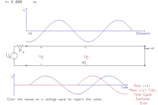
sinusoidal with time, as well. In the
above drawing, t=6 ns and the leading edge of the sinusoid is about to arrive
at the load. The short circuit will
reflect the sinusoid with an amplitude of –5 volt, and then the wave on the
transmission line with be the sum of a positive-going sinusoid with a 5 volt
amplitude, and a negative-going sinusoid with an amplitude of –5 volts. (Strictly speaking, the “amplitude” should
be a positive number so we should speak of an amplitude of 5 volts and a phase
of 180 degrees!)
At t=9 ns, the reflected wave has traveled
back along the line for about 1/3 of the line length, and there is a sharp
discontinuity in the slope of the voltage as a function of distance at the
leading edge of the reflected wave. The
reflected wave has not yet arrived at the V2 voltmeter location.
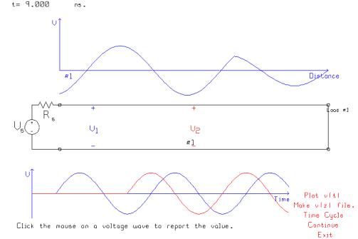
At t=11 ns, the reflected wave has propagated
past the V2 location and so at V2 the net voltage is equal to the incident plus
the reflected wave. At the V2 location the reflected wave is exactly out of
phase with the incident wave, and so the incident and reflected wave add up to
zero! Note that the red curve in the
voltage vs. time graph has become equal to zero near the right hand edge of the
graph. The reflected wave has not yet
reached the V1 location, however.
In this graph
the time has advanced to 18 ns and the reflected wave has arrived at the V1
location. At V1, the incident wave and the reflected wave are exactly in phase,
so the two waves add up to a sinusoid of amplitude 10 volts. We see the amplitude of V1 in the voltage
vs. time graph increase abruptly from 5 volts to 10 volts.
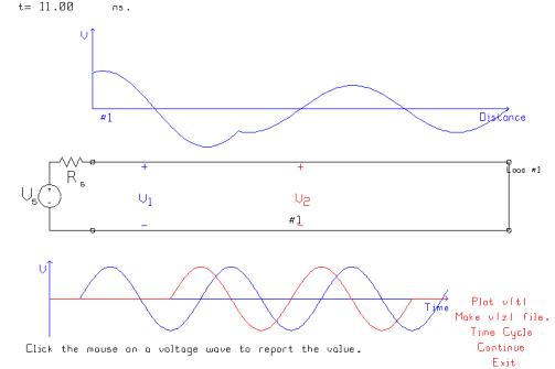
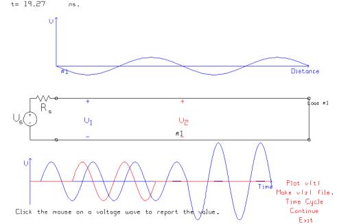
Let
time advance further. Notice that the
voltage wave on the transmission line does not slide along the line from left
to right. Instead, the wave “marches in
place”, and is called a “standing wave”.
This can be shown by looking at the voltage on the line at
closely-spaced time instants.
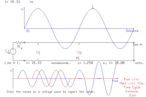
At 18.33
ns, the sinusoid on the transmission line has the maximum possible amplitude of
10 volts. As time increases the
amplitude of the wave decreases but the positions of the maxima and of the zero
crossings do not move.
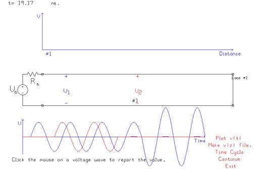
At 19.17
ns, the incident and the reflected wave exactly cancel out everywhere on the
line, and so the voltage on the transmission line is momentarily equal to zero
everywhere.
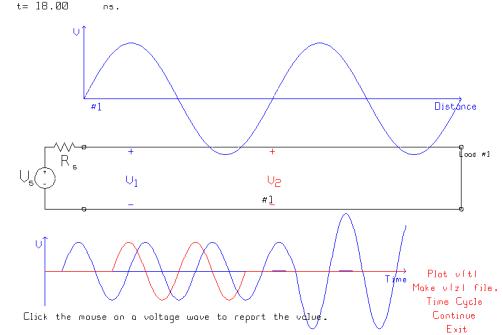
As we let
time increase further, the voltage rises, reaching a maximum a quarter of a
period later. If the load is changed to
an open circuit, the reflection coefficient is +1 and the reflected wave is
again equal and opposite to the incident wave.
The same standing wave behavior is seen.
Set the load to 100 ohms, so that the
reflection coefficient is +1/3. Then we
expect a reflected wave of amplitude 1.667 volts. The voltage on the transmission line is then the sum of a wave
traveling the right of amplitude 5 volts and a wave traveling to the left of
amplitude –1.667 volts. The two waves
are in phase at some locations, and add up to make a sinusoid of amplitude
6.667 volts. At other locations, the
waves are out of phase, and subtract, to make a sinusoid of amplitude 3.333
volts.
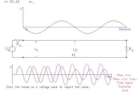
This
graph shows the voltages at 23.33 ns.
At the V1 observer, we see an initial sine wave of amplitude 5
volts. Then when the reflected wave
arrives, the amplitude decreases to 3.333 volts. At the V2 location, the initial amplitude is 5 volts, but when
the reflected wave arrives the amplitude increases to 6.667 volts. At t=23.33 ns, the voltage on the
transmission line as a function of distance is a minimum. Let time advance some more.
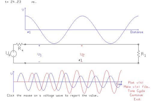
At 24.23
ns, the voltage on the transmission line as a function of distance is 6.667
volts, the largest that it gets. As
time advances the wave slides along the transmission line but not at a uniform
speed. The amplitude changes as the
wave slides along. The maximum
amplitude is 6.667 volts as shown here, and the minimum is 3.333 volts.
9
Capacitive
Termination
Return to the simplest transmission line
circuit consisting of a step generator of 50 ohm internal resistance, and a
transmission line of length 2 m, characteristic resistance 50 ohms, and wave
speed 300 meters/microsecond. Change
the load termination to a capacitor of capacitance 10 pF, in parallel with a
100,000 ohm resistor. The BOUNCE program considers this large resistance to be
an open circuit so the load terminating the transmission line is a 10 pF
capacitor.
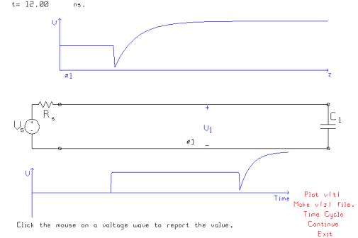
The generator is a step of height
10 volts, with a 50 ohm internal resistance operating into a 50 ohm line. So the voltage divider puts 5 volts onto the
line. The observer V1 near the middle
of the transmission line sees the voltage step up to 5 volts when the leading
edge of the step function arrives. The
step function then travels on to the load.
The capacitor is initially uncharged, so the initial condition is that
the load voltage is equal to zero. Zero
volts behaves momentarily like a short circuit, with a reflection coefficient
of –1, so the reflected wave initially has an amplitude of –5 volts. As time goes by the capacitor charges with a
time constant ![]() , equal to the
characteristic resistance of the transmission line,
, equal to the
characteristic resistance of the transmission line, ![]() , times the capacitance,
, times the capacitance, ![]() As time goes by the
capacitor becomes fully charged, and zero current flow, which behaves like an
open circuit, with reflection coefficient +1.
So after a long time the reflected wave has amplitude +5 volts. So initially the reflected wave has
amplitude –5 volts, then “charges” exponentially with a time constant equal to
As time goes by the
capacitor becomes fully charged, and zero current flow, which behaves like an
open circuit, with reflection coefficient +1.
So after a long time the reflected wave has amplitude +5 volts. So initially the reflected wave has
amplitude –5 volts, then “charges” exponentially with a time constant equal to ![]() to a final value of
+5 volts.
to a final value of
+5 volts.
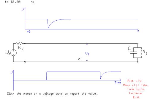
In the figure shown above the
observer at V1 sees the “incident” step function of height +5 volts arrive, and
then the voltage remains at +5 while the step travels to the capacitor. There it is reflected with an initial
reflection coefficient of –1, so the leading edge of the reflected wave has
amplitude –5 volts. When the
reflection arrives at the observer at V1, the voltage is the sum of the
incident voltage, +5, plus the reflected voltage, -5, adding up to zero
momentarily. Then as time goes by the
reflected wave changes exponentially from –5 to +5 volts, so the net voltage
changes exponentially from zero to +10 volts. The final value of the voltage at
V1 is +10 volts.
Thus an uncharged capacitor
behaves initially as a short circuit load, but after a long time behaves as an
open circuit load.
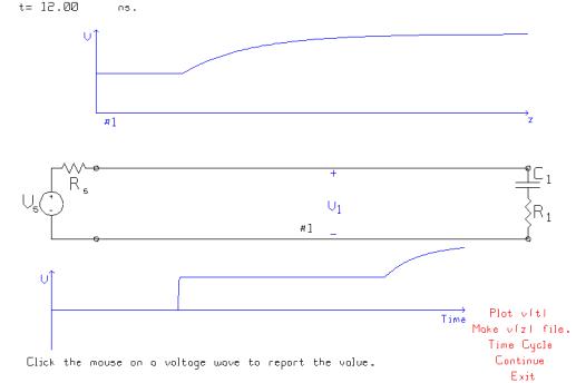
Change the circuit so that the resistor in
parallel with the capacitor is 50 ohms.
When
the step function arrives at the load, the capacitor is initially uncharged, so
behaves as a short circuit. This “reflects” a voltage of initial amplitude –5
volts. As time goes by and the
capacitor charges, it becomes an open circuit.
The net load is thus an open circuit in parallel with a 50 ohm resistor,
which amounts to a matched load. Thus
the reflection coefficient is zero and the “final” value of the reflected wave
is 0 volts. The reflected wave thus
changes exponentially from an initial value of –5 volts to a final value of
zero volts. The time constant is the
capacitance times the resistance that it “sees” across its terminals. This is
the parallel combination of the load resistor and the characteristic resistance
of the transmission line.
Change
the load to a series combination of a 50 ohm resistor and a 10 pF capacitor.
In
this case, the uncharged capacitor initially behaves as a short circuit, and so
the termination is a 50 ohm resistor which matches the transmission line. The initial value of the reflection
coefficient is zero. As time goes by the
capacitor charges, and the current drops to zero, and so the capacitor behaves
as an open circuit. The reflection
coefficient is then +1 and the final value of the reflected wave is +5 volts.
Thus at the V1 observer, the voltage steps up to +5 volts, then when the
reflected wave arrives, increases exponentially to +10 volts. The time constant is the capacitance times
the resistance at the capacitor terminals, equal to the load resistor in series
with the line’s characteristic resistance.
10 Inductive Load
Consider
a transmission line circuit with a step function generator of amplitude 10
volts and internal resistance 50 ohms. The line is 2 m long with characteristic
resistance 50 ohms, and speed of propagation 300 meters per microsecond. Choose a series RL load, and set the load
resistance to zero ohms. Choose a 10
nanoHenry inductance.
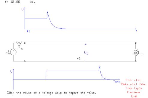
The observer at V1 sees a step
function of +5 volts when the leading edge of the generator voltage arrives at
the V1 location. The inductor has zero
current initially, so behaves as an open circuit initially, with a reflection
coefficient of +1. The reflected wave
has an initial value of +5 volts, so when the reflected wave arrives at the V1
location, the voltage there rises momentarily to +10 volts. As time goes by the current in the
inductance builds up to a constant value and the voltage across it falls to
zero volts, like a short circuit. Thus as time goes by the reflection
coefficient becomes –1 and the reflected wave amplitude becomes –5 volts. The net voltage at the V1 location thus
declines exponentially to zero. The
time constant is R/L, where R is the resistance seen at the inductor terminals,
equal to the characteristic resistance of the transmission line.
Change the resistance in series with the
inductor to 50 ohms.
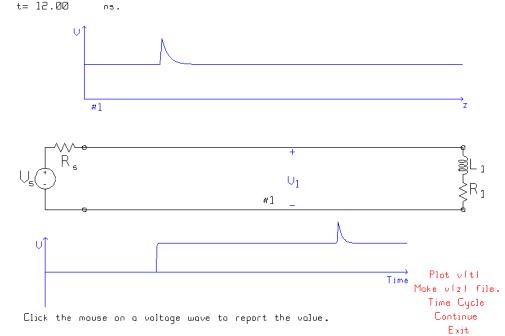
The inductor initially behaves as
an open circuit with a reflection coefficient of +1, so the initial value of
the reflected wave is +5 volts, and the voltage at the V1 location rises
momentarily to +10 volts. As time goes
by the current in the inductor builds up and the inductor becomes a short
circuit. The load terminating the line
is then the R1 resistor, which is a match, with zero reflection
coefficient. Thus the final value of
the reflected wave is 0 volts. The
voltage at the V1 location declines exponentially from +10 to +5 volts. The time constant is R/L, where R is the
resistance seen from the inductor terminals, equal to the R1 resistor in series
with the characteristic resistance of the transmission line.
Change the load circuit to a parallel RL
circuit, with a 50 ohm resistor in parallel with a 10 nanoHenry inductance.
In this circuit, the inductor is
initially an open circuit, so the load initially behaves as a 50 ohm resistor,
which is a match, so the initial value of the reflected wave is zero. As time
goes by the inductor current builds up to a constant value, and so the voltage
across the inductor becomes zero. Zero volts is like a short circuit with
reflection coefficient –1, so the final value of the reflected wave is –5
volts. At the V1 location, the voltage
starts as +5 volts, and declines exponentially to 0 volts. The time constant is the parallel
combination of the R1 load with the characteristic resistance of the line,
divided by the inductance.
11 Junction Reflection Problem
This section considers a transmission line problem having a junction of two transmission lines. The problem is such that pulses arrive at the junction simultaneously from the left and from the right and so care must be taken in working out the net reflections on either side of the junction.
A generator produces a pulse 2 ns wide of amplitude 10 volts, open circuit. The generator’s internal resistance is 25 ohms. The generator drives a 50 ohm line of length 2 m, which is connected in series with a 100 ohm line of length 2 m. Both lines have propagation speeds of 30 cm/ns. The 100 ohm line is terminated with a 50 ohm resistor. Find the voltage on the two transmission lines at t= 21.37 ns.
The “transit time” of each transmission line is 200 cm / ( 30 cm/ns ) = 6.667 ns, so 21.37 ns is time enough for a little more than three trips along each line. On the first trip, the source’s pulse reaches the junction and is partially reflected and partially transmitted. On the second trip, the reflected pulse is re-reflected from the generator, and the transmitted pulse is reflected from the load. On the third trip these two pulses arrive at the junction simultaneously, and the problem is to use the reflection and transmission coefficients at the junction to work out the correct resultant pulse on line #1 and on line #2. Students should solve this problem with a “bounce diagram”[4] and then use BOUNCE as a laboratory to verify their solution step by step.
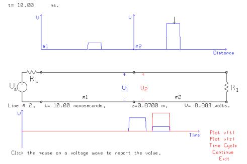
Arrange a “voltmeter” 20 cm from the junction on line #1, and similarly 20 cm from the junction on line #2. These voltmeters “observe” the amplitude of the pulses as they go past. The initial pulse incident on the junction from the generator has an amplitude of 10 x 50/75 = 6.667 volts. The first reflection from the junction has amplitude 6.667 x (100-50)/150 = 2.222 volts; the first transmission through the junction has amplitude 6.667x 200/150 = 8.889 volts. These values can be “read back” from bounce by letting the program run to advance the time to 10 ns, then clicking the mouse on the voltage waveforms. Thus in the above figure the program reports that the amplitude of the transmitted pulse is 8.889 volts.
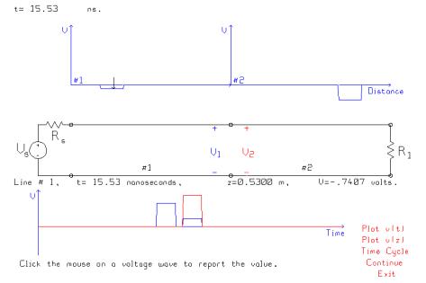
Next let time advance until the pulse traveling to the left on line #1 is reflected from the generator, and the pulse traveling to the right on line #2 is reflected from the load. In the figure above the time is 15.53 ns, and the pulse reflected from the generator is being “read back” as of amplitude –0.7407 volts. The reflection coefficient at the generator is –1/3, so the reflection is expected to have amplitude 2.222 x (-1/3) = -0.7407 volts, in agreement with the BOUNCE simulation. The first reflection from the load has amplitude 8.889 x (50-100)/150 = -2.963 volts, which can be verified to agree with BOUNCE’s value.
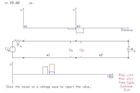
Allowing time to advance to 20 ns brings the two pulses to the junction, and the figure shows that both pulses arrive at the junction simultaneously. To calculate the interaction at the junction, consider the pulses individually and add up the results. Thus, due to –0.7404 volts arriving from the left, the reflected pulse has amplitude -0.7407 x 50/150 = -0.2469 traveling to the left, and the transmitted pulse has amplitude -0.7407 x 200/150 = -0.9876 traveling to the right. Due to the –2.963 volt pulse arriving from the right, the reflected pulse amplitude is-2.963 x 100/150 = +0.9877 traveling to the right, and the transmitted amplitude is -2.963 x 100/150 = -1.975 traveling to the left. Adding up these values obtains a net pulse traveling to the right of amplitude -0.9876 +0 9877 = 0.001 volts, and a net pulse traveling to the left of -0.2469 –1.975 = -2.222 volts.
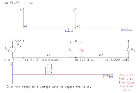
We see that the pulse traveling to the left from the junction has amplitude –2.222 volts. There is no pulse transmitted to the right, or more correctly the wave transmitted through the junction and the wave reflected from the junction cancel on transmission line #2.
12 Terminating a Computer Bus
Consider a logic gate, represented by its
Thevenin equivalent voltage soruce ![]() and internal
resistance
and internal
resistance ![]() , driving a transmission line of length
, driving a transmission line of length ![]() , characteristic resistance
, characteristic resistance ![]() , and speed of propagation
, and speed of propagation ![]() . The line is
terminated with a CMOS gate having a high input resistance and an input
capacitance
. The line is
terminated with a CMOS gate having a high input resistance and an input
capacitance ![]() , as shown in the figure below.
, as shown in the figure below.
When can the transmission line be considered
as a “lumped” circuit element, and when does “distributed” circuit analysis
have to be used? If the rise time of
the generator from “0” to “1” is ![]() seconds, then the
length of the rising edge on the transmission line is
seconds, then the
length of the rising edge on the transmission line is![]() meters. The “rule of
thumb”[2,3] is that if the length of the transmission line
meters. The “rule of
thumb”[2,3] is that if the length of the transmission line ![]() is less than 1/6 of
the length of the rising edge, then the problem can be solved by lumped circuit
analysis, but if
is less than 1/6 of
the length of the rising edge, then the problem can be solved by lumped circuit
analysis, but if ![]() , then the problem must be solved using distributed circuit
analysis. Thus solve the circuit as a
transmission line if
, then the problem must be solved using distributed circuit
analysis. Thus solve the circuit as a
transmission line if
![]()
The
following investigates a transmission line problem for various values of the
rise time.
Consider a CMOS digital driver changing state
from zero (0 volts) to one(five volts).
Typical values[2] for the characteristics of a CMOS gate output are that
the 10 to 90% rise time is 4.7 ns, the output resistance in the “low” state is
37 to 83 ohms and in the “high” state is 45 to 165 ohms, and the minimum output
voltage for a logical “1” is 3.8 volts.
To illustrate the behavior, the source resistance will be taken as a
middle value, say 75 ohms. The input
characteristics of a CMOS logic gate might typically be a high resistance, a
capacitance of 3.5 pF, and a minimum voltage for the gate to reliably switch to
“logical 1” of 3.8 volts.
Consider a logic gate driving a transmission
line of 10 cm length, terminated with a CMOS gate input. The line might have a characteristic
resistance of 50 ohms and a speed of propagation of 14 cm/ns. We wish to determine the 90% rise time at
the input to the logic gate, which is the time required for the voltage to rise
to 4.5 volts and remain above that value.
A transmission line having propagation
velocity ![]() m/s and
characteristic resistance
m/s and
characteristic resistance ![]() ohms has capacitance
per unit length
ohms has capacitance
per unit length
![]() F/m
F/m
With ![]() =140 m/microsec and
=140 m/microsec and ![]() =50 ohms, c=142.8 pF/m and a 10 cm line has capacitance 14.28
pF. The “lumped circuit” view of this
problem puts the 14.28 pF capacitance in parallel with the 3.5 pF CMOS input
capacitance, for a total of
=50 ohms, c=142.8 pF/m and a 10 cm line has capacitance 14.28
pF. The “lumped circuit” view of this
problem puts the 14.28 pF capacitance in parallel with the 3.5 pF CMOS input
capacitance, for a total of ![]() 17.8 pF. The time
constant of the generator resistance of
17.8 pF. The time
constant of the generator resistance of ![]() ohms and the net
capacitance is
ohms and the net
capacitance is ![]() 1.33 nS. If we assume
zero or negligible rise time for the source, then the 90 percent rise time of
an exponential rise with this time constant is 3.07 ns. If the generator is modeled as a ramp from
0 volts to 5 volts in 4.5 nS, then the 90% rise time is 5.9 ns.
1.33 nS. If we assume
zero or negligible rise time for the source, then the 90 percent rise time of
an exponential rise with this time constant is 3.07 ns. If the generator is modeled as a ramp from
0 volts to 5 volts in 4.5 nS, then the 90% rise time is 5.9 ns.
It
is of interest to compare this “lumped circuit” result with the “distributed
circuit” result for various rise times of the source.
12.1 Response With a Short Rise Time
The simplest model of this circuit is to
represent the CMOS output as a step function generator stepping up from 0 to 5
volts with zero rise time. The one-way
transit time is 10/14 = 0.714 ns, so in a simple-minded view we might expect
the voltage at the gate to step up at 0.714 ns. However, mismatch increases the 90% rise time substantially above
this figure because the initial step at the logic gate input is not as large as
4.5 volts.
The shortest rise time available in the
BOUNCE program is one time step; this is conveniently set at 5 ps for this
problem. At ![]() =140 m/microsec, the length of the rising edge is only 0.07
cm and so clearly with such a fast rise time, the circuit should be solved with
distributed circuit analysis.
=140 m/microsec, the length of the rising edge is only 0.07
cm and so clearly with such a fast rise time, the circuit should be solved with
distributed circuit analysis.
The
initial step applied to the line is 5x50/(50+75)=2 volts. After 0.715 ns, the leading edge arrives at
the load, and the voltage steps up to 4 volts.
This is larger than the minimum of 3.7 volts for a “logical 1”, but it
is not larger than 4.5 volts so we must permit time to advance to determine the
90% rise time.
After
about 1.4 ns, the source re-reflects the voltage, and the voltage on the line
steps up to 4.4 volts. This step
travels back to the load, arriving at about 2.14 ns.
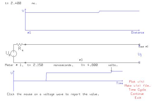
At 2.150
ns, the load voltage steps up to 4.8 volts.
So the “90% rise time” is 2.15 ns, about three times the transit time of
the transmission line, and the fundamental reason for this long time is the
mismatch between the 75 ohm generator resistance and the 50 ohm line
characteristic impedance. The range of
generator impedance values quoted in Ref. [1] is 45 to 165 ohms, so in the
worst case the mismatch problem is much more severe.
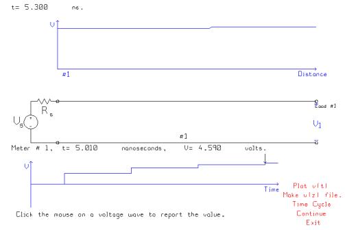
This
graph shows the voltage at the load when the generator resistance is the ‘worst
case’ value of 165 ohms. The voltage
rises to 2.325 volts, then steps up to 3.569 volts, then 4.234 volts and finally
4.590 volts at 5.010 ns. The second
step, to 3.569 volts, just misses the minimum for a “logical 1”. The fourth step exceeds 4.5 volts so the
“90% rise time” is 5.01 ns, much longer than 2.15 ns with a 75 ohm generator
resistance.
12.2
Including
the Gate Input Capacitance
The gate terminating the transmission line
has an input capacitance of 3.5 pF. How
does this change the response with a 75 ohm generator resistance? Initially the capacitance is uncharged, with
zero volts across it. When the initial
2 volt step from the generator arrives, the capacitor charges gradually towards
a final value of 4 volts.
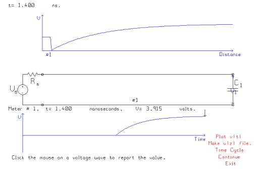
After
0.715 ns, the leading edge of the generator’s 2 volt step arrives at the
load. The capacitor is uncharged, and
so behaves as a short circuit. As time
goes by the capacitor becomes an open circuit with a reflection coefficient of
+1, so charges towards 4 volts. At
t=1.400 ns, the reflection from the uncharged capacitor is moving to the left
and will soon be reflected from the unmatched source. At the load, the voltage has risen to 3.915 volts.
A short time later the transient is reflected from the source and is seen
as a small step downward traveling to the right towards the load.
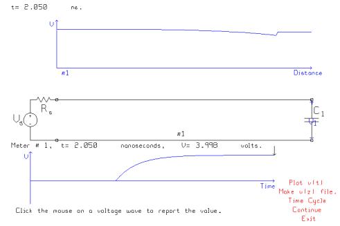
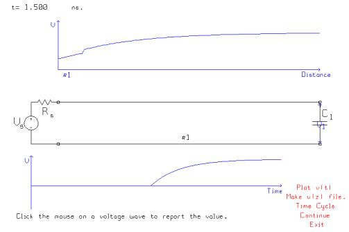
At
t=2.050 ns, we see the small downward step is about to arrive at the load. The step down is followed by an upward trend
in the voltage on the transmission line.
When the small downward step arrives at the load, the voltage across the
load initially declines by a small amount.
Then the load voltage rises in response to the rising voltage arriving
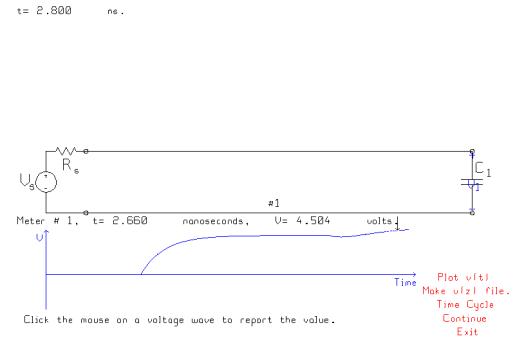
from the generator. At 2.660 ns, the
voltage exceeds 4.5 volts, and so the 90% rise time is 2.66 ns. This is longer than the value of 2.15 ns
found by neglecting the input capacitance.
The CMOS gate’s input capacitance thus slows down the circuit.
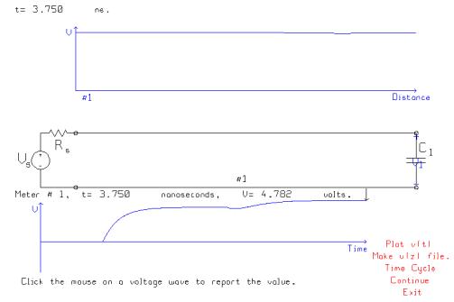
After further time passes the voltage on the line and at the load
gradually stabilizes to 5 volts.
Thus including the input
capacitance of the CMOS gate terminating the line, the 90% rise time is
estimated as 2.66 ns, which is somewhat shorter than the “lumped”
circuit answer of 3.07 ns for an abrupt step function generator.
12.3
With
1 ns Source Rise Time
The rise time of typical CMOS logic is 4.5 ns. To illustrate the changes in the response when the step function does not rise abruptly, first we will look at the response with a 1 ns rise time and then with a 4.5 ns rise time.
Consider the logic circuit having a 75-ohm generator that rises from 0 to 5 volts in 1 ns. The length of the rising edge is 14 cm, and limiting length of transmission line for which “lumped” circuit analysis should be used is 2.3 cm. Thus our 10 cm transmission line should be solved as a distributed circuit.
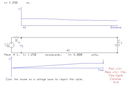
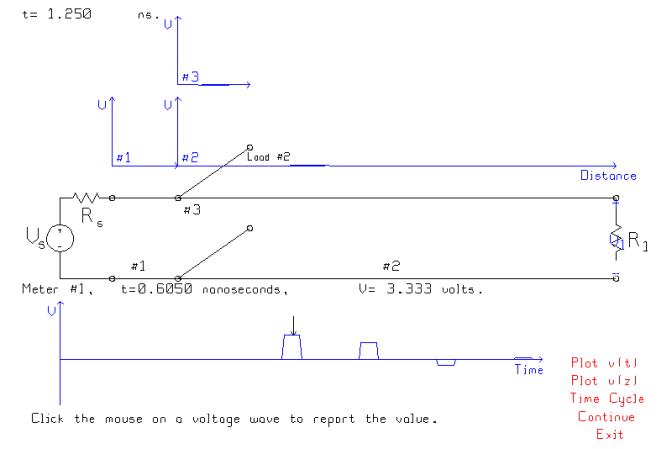
This figure shows a voltmeter at the source, with the voltage as a function of time at the bottom of the figure. The source rises from 0 to 5 volts in 1 ns. The leading edge of the voltage as a function of distance on the transmission line is a ramp of length 14 cm, longer than the 10 cm length of the whole transmission line. At t=1.25 ns, the voltage at the source has risen to its maximum value of 2 volts, and the leading edge of the ramp has reached the load capacitor which has begun to charge.
12.4
With
4.5 ns Source Rise Time
The figure quoted in Ref. [2] as a “typical” rise time for CMOS is 4.5 ns. The length of the rising edge on the transmission line is 63 cm, and the limiting transmission line length for which lumped circuit analysis can be used is 1/6 of this, or 10.5 cm. So the 10 cm transmission line in our example could be solved with lumped circuit analysis for this “slow” rise time.
The voltage at the load “ramps up” in response to the linear increase in the source voltage. The voltage-vs.-distance graph at the top shows that the voltage is almost the same at all points on the transmission line, suggesting that the delay times associated with the transmission line are not significant compared to the slow rate of increase of the source voltage. The load voltage exceeds 4.5 volts at t=5.5 ns so this is the 90% rise time.
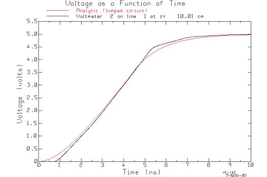
This graph compares the analytic solution to the problem (red curve), which approximates the transmission line with a lumped capacitor equal to the capacitance per unit length times the length. The 90% rise time for the analytic curve is 5.9 ns. The black curve is the voltage at the load calculated with BOUNCE. There is a time delay of 0.7 ns as the leading edge of the generator’s ramp voltage travels from the generator to the load. Then the load voltage rises nearly linearly with time, an the analytic curve agrees quite well with the transmission line model. After about 5 ns the voltage predicted by the transmission line model exceeds the lump circuit approximation. The voltage rises above 4.5 volts in 5.5 ns, more quickly than the 5.9 ns of the analytic model. This transmission line’s length is approximately 1/6 of the length of the rising edge of the source voltage. This is an example of the longest transmission line circuit that should be approximated by lumped circuit analysis. The figure shows that there is some error incurred in the lumped circuit approximation.
13 Notes About Approximation
BOUNCE does not provide an exact solution to the transmission line
equations. Like many methods in
computational electromagnetics, BOUNCE divides time into steps of ![]() and space into cells
of size
and space into cells
of size ![]() , and obtains an approximate solution to the equivalent
“discretized” problem. The finer the
discretization, the more accurate the solution, within the limits of the
accuracy of the single-precision arithmetic that the program uses.
, and obtains an approximate solution to the equivalent
“discretized” problem. The finer the
discretization, the more accurate the solution, within the limits of the
accuracy of the single-precision arithmetic that the program uses.
BOUNCE uses a very simple shift-and-add algorithm to keep track of
the positive-going travelling wave and the negative-going travelling wave on
each transmission line at each time step.
BOUNCE must use the same time step on all the transmission lines; hence
the distance traveled by the wave in one step on each line must be the
propagation velocity ![]() times the time step
times the time step ![]() , which is the “cell size”
, which is the “cell size” ![]() for that line. The nearest integer number of cells
approximates the length of each transmission line. Hence BOUNCE does not solve the problem exactly, but instead
rounds the line lengths off to the nearest whole number of cells. Using a smaller time step reduces the error
in approximating the line lengths but also slows down the animation. The animation works well when there are 100
to 200 cells in total.
for that line. The nearest integer number of cells
approximates the length of each transmission line. Hence BOUNCE does not solve the problem exactly, but instead
rounds the line lengths off to the nearest whole number of cells. Using a smaller time step reduces the error
in approximating the line lengths but also slows down the animation. The animation works well when there are 100
to 200 cells in total.
Pulses and step functions in BOUNCE are not perfectly square. A step or a “square” pulse rises linearly from zero to its full amplitude in one time step. Thus steps and pulses have a “rise time” of one time step. The fall time back to zero is also one time step.
BOUNCE solves a first-order differential equation at RL or RC loads, to find the reflected voltage at the next time step given the incident voltage.
14 References
[1] C.W. Trueman, “BOUNCE User’s Guide”, Electromagnetic Compatibility Laboratory, Concordia University, November 1, 2001.
[2] H.W. Johnson and M. Graham, “High-Speed Digital Design – A Handbook of Black Magic”, Prentice-Hall, 1993
[3] S.H. Russ, “Electromagnetic Effects in High-Speed Digital Systems”, Chapter 10 in J.D. Kraus and D.A. Fleisch, “Electromagnetics With Applications”, McGraw-Hill, 1999.
[4] C.R. Paul, K.W. Whites and S.A. Nasar, "Introduction to Electromagnetic Fields,", 3rd edition, McGraw-Hill 1998.
C.W. Trueman