 |
|
|
|
|
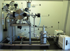
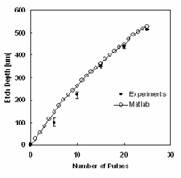
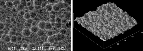
Micromachining/Microfabrication George-Avinash-Arvind-Kiran Development of different microfabrication techniques for Silicon and piezoelectric materials. Silicon fabrication includes the characterization of photolithography process, Oxide etching and characterization (for oxidised wafers), isotropic etching with Xenon Difluoride and Anisotropic etching with alkali etchants, Suitable post-processing and packaging techniques. Isotropic etching The rapid progress in Micro-Electro Mechanical Systems necessitated the development of a micromachining technique in order to release micro-mechanical device in integrated chips. In the late 1990s there was a quest for a dry etchant, that would not require an expensive setup, and overcome the problems related to wet etching, such as, stiction and etching slowdown due to bubble formation. A good alternative to wet etching would have been plasma etching, but fine tuning of the process parameters to achieve an effective control of the process, combined with the expensiveness of the equipment made plasma etching a less affordable etching method for many small labs. In gaseous phase, xenon difluoride was found to etch silicon isotropically and the required process setup is quite simple compared to other isotropic etching equipment for silicon. At the Optical- Bio,Microsystems Laboratory, a new and computer-controlled xenon difluoride etching equipment for silicon was designed and installed. Using the designed and fully in house built etching equipment, experiments were carried on silicon samples. The equipment, as designed and built, has embedded safety features required by toxic gas handling equipment codes.
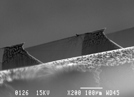
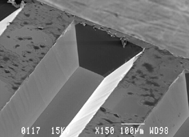
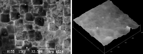
Anisotropic etching The anisotropic etching of silicon is a vastly explored yet fascinating area of study. Several unique features on Silicon can be created by taking advantage of the anisotropic etching behavior of Silicon when introduced with wet chants such as Tetra Methyl Ammonium Hydroxide (TMAH), Potassium Hydroxide (KOH),etc. The research at the Optical -Bio Microsystems Laboratory on Anisotropic micromachining is carried out as a part of device fabrication for microfluidic and micromechanical devices. Etch characterization is carried out in order to study the etch rate, under etch rate, and the variation of etch parameters with different physical conditions.
A hybrid micromachining technique suitable for reducing surface roughness for different microsystems is carried out. Influence of surface roughness on on the performance of microsystems is very important in order to obtain the predicted behavior. While unconstrained geometry of micromachining is realised with isotropic etching, the purpose of anisotropic etching is to smoothen the rough surface of the etched sample utilizing the selectivity of anisotropic etchant for different crystal planes. Thus, by carefully combining the isotropic etching along with controlled anisotropic etching of the sample, it is possible to improve and tune the surface roughness of the etched sample for obtaining optimal performance. Using this micromachining technique, a clear improvement in surface roughness has been observed by experimental characterization of the roughness parameters using Scanning Electron Microscope (SEM) and Atomic Force Microscope (AFM) measurements.
|
|
|
|