INTRODUCTION
This tutorial is an introduction to the Layout Editor available from
the Cadence design tools (Design Framework II) and the CMOSIS5 design kit
from the Canadian Microelectronics Corporation (CMC). This tutorial
is based on version Cadence 97a of the Cadence software
tools.. The CMOSIS5 design kit is based on the Hewlett-Packard CMOS14TB
process. This is a high-speed, high density 0.5 micron CMOS process
which features a 0.6 micron drawn gate length optimized for 3.3 V operation.
The CMOS14TB process is a triple-metal, single poly CMOS process.
The tutorial guides the user through a complete hierarchical design
and simulation of a CMOS inverter circuit. The
inverter is constructed using NMOS and PMOS transistors. The
transistors are first created as cells within a specific design library.
Following this, a new cell (the CMOS inverter) is created using instances
of the previously created NMOS and PMOS cells.
Following a Design Rule Check, the a symbol view for the inverter is created. This symbol view of the layout will then be used to create a testbench schematic (complete with a DC power supply and input stimuli ). The testbench will then be simulated to verify correct operation of the inverter and to obtain its performance characteristics (i.e. rise and fall times).
Some of the commands given in this tutorial are specific to the setup we have here at Concordia University. Contact your system administrator for information pertaining to your environment.
I: USING THE VIRTUOSO LAYOUT EDITOR TO CREATE A PMOS TRANSISTOR
This section will explore the use of the Virtuoso Layout editor. A p-type
MOS transistor will be
designed. A p-type MOSFET transistor is fabricated with the CMOS14TB
process by crossing
polysilicon and N-Island in a P-Substrate.
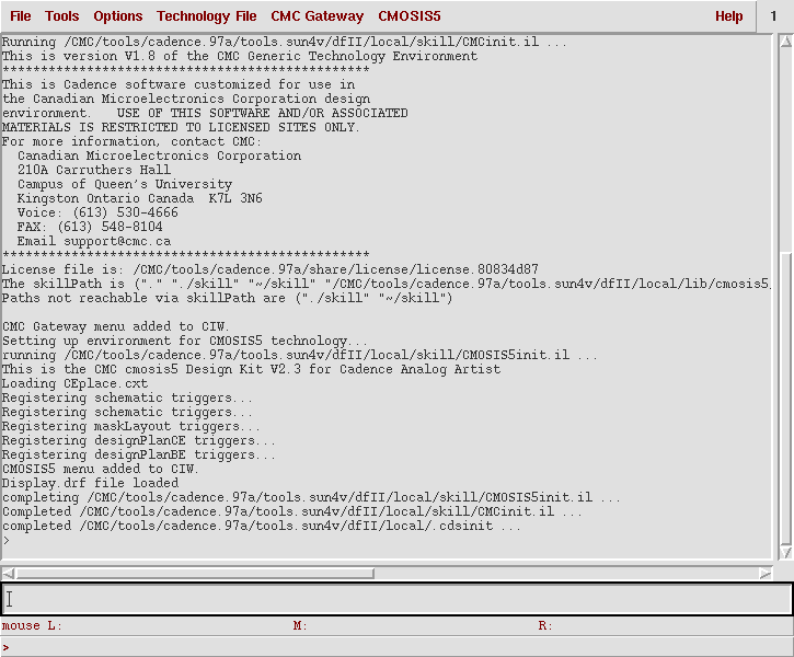
1-1: Start the Cadence tools by typing the following command from the UNIX prompt:
% cmosis5
The main CIW (Command Interpreter Window) will appear as shown in the following figure:
1-2: To create a new library and attach it to the CMOSIS5 technology
file select: File -> New ->
Library. The New Library window will appear.

In this window fill in the following: Name: mylib (or any other suitable
name), Technology File: select the Attach to an existing techfile button.
Select OK at the top of the New Library window by left clicking with the
mouse. Once you have one this, a new window will appear. This is
the Attach Design Library to Technology File as
shown in Figure 1 below:
