Several data transmission
standards require phase-locked loops (PLLs) with well controlled
bandwidth and peaking characteristics. To allow flexibility in the
setting of these two loop parameters, dual-path PLLs have been
demonstrated, using LC voltage-controlled oscillators (VCOs) [1].
Although LC VCOs have superior phase noise performance for a given
power dissipation as compared to ring-based VCOs, the use of inductors
limits their integration into a standard microprocessor design flow and
significantly increases their chip area. If the system’s jitter
requirements allow for a ring VCO the resulting PLL will be smaller and
have less affect on the design flow of the rest of the chip. With these
benefits in mind, this project considers the relationship between PLL
bandwidth and VCO gain for ring VCOs, and demonstrates the
effectiveness of a technique for maintaining near-constant VCO gain
across the tuning range.
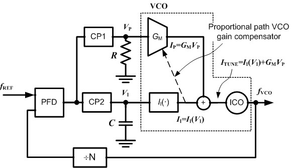
Fig. 1: Dual path PLL. Dashed line depicts the proposed linearization technique.
Fig. 1 shows a dual path PLL
consisting of two charge pumps, CP1 and CP2, and two loop filters. CP1
drives a resistor to develop a voltage, VP, that is proportional to the phase difference between the reference signal, fREF, and a divided version of the output signal, fVCO. Similarly, voltage VI is based on the integral of the output of the phase frequency detector denoted by PFD. Voltages VI and VP
are converted to currents within the dual-path VCO and applied to the
current-controlled oscillator (ICO). Given certain assumptions about
the PLL’s loop dynamics, the bandwidth is proportional to the
proportional path’s VCO gain KP. Assuming GMP is constant, KP
and the PLL’s bandwidth may vary significantly as the VCO is
tuned. For a delay interpolating VCO with a 1:2 tuning range, KP will have a 1:4 range.
A proposed solution [2] for reducing KP’s variation is to set GMP as a function of state of the integral tuning path, by using the integral path to control the bias for the transconductor GMP. Simulation results have shown a significant reduction in across-band variation in KP. Measurements of a test chip designed and fabricated in STMicroelectronics 90nm technology are underway.
[1] A. L. S. Loke, R. K. Barnes, T. T. Wee, M. M. Oshima, C. E. Moore, R.R Kennedy, and M. J. Gilsdorf, “A versatile 90-nm CMOS charge-pump PLL for SerDes transmitter clocking,” IEEE J. Solid-State Circuits, vol. 41, no. 8, pp. 1894-1907, Aug. 2006.
[2] G. Cowan, D. Friedman, M. Meghelli, “Architecture for maintaining constant voltage controlled oscillator gain,” U.S. Patent 7741919. Issued June 22nd, 2010.